© IMEC
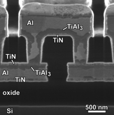
| | FIB cross-section through a hot Al via chain © IMEC | |
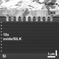 | Cross-sectional FIB image through a Cu damascene trench structure in a SILK (Dow Chemical) dielectric on top of a stack of 10 dual-layers oxide hard mask/SILK. © IMEC | |
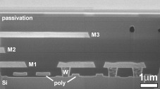 | FIB cross-section through a 4-layer metal device. © IMEC | |
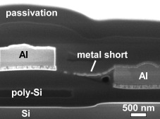 | Cross-sectional FIB image through a failure site showing the presence of a metal short between the two Al lines. © IMEC | |
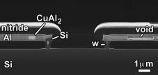 | Electromigration test structure showing the formation of a void on the cathode and the accumulation of Si and Cu on the anode side. © IMEC | |
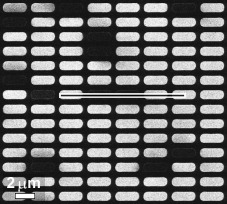 | ||
 | Voltage contrast reveals open via positions in a contact chain structure. The cross-section image at the position of the line shows too undeep etching of the vias. © IMEC | |
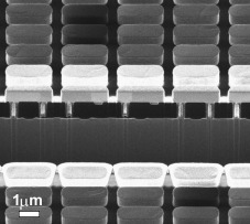
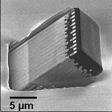
 | Tilted view of a specimen for transmission electron microscopy prepared by the FIB trench milling procedure through a 5-layer metal via chain test structure. © IMEC | |
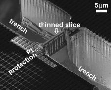
 | Liftout sample of a DRAM. The sample was cut out of the wafer with FIB, transferred to a carrier with a micromanipulator and glued tight by heating. After further FIB polishing two perpendicular sides of the sample can be imaged. This technique allows wet chemical preparation like lift-off or staining and high-resolution imaging in the SEM. © Infineon | |
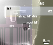 | Modifications on a three-layer metal structure. The layout is overlaid on the top view FIB image taken after the modification (M1 pink, M2 blue, M3 yellow). © IMEC | |